Methods Used in PCB Assembly
PCB assembly completes the physical building of a circuit board by picking, placing, and soldering components to the bare circuit board. This is done through the use of pick-and-place and reflow technology to place components on the board and make secure electrical connections. Using these advanced technologies enables manufacturers to deliver high-quality electronic products while remaining cost-effective.
Modern PCB assembly methods provide significant benefits in terms of efficiency, precision, and reliability. Enhanced automation reduces reliance on manual labor and eliminates the potential for human error that can hamper production timelines and overall quality. Additionally, these innovations offer lead-free options that align with environmental regulations while maintaining robust electrical connections.
The initial step in the assembly process is to prepare the bare board assembly for component placement. This involves applying a thin layer of copper foil to both sides of the board. The copper is then covered by a solder mask, which provides places to attach components, and a silkscreen, which includes labels for each component and its function.
The next step in the process is to mount the components on the bare board through the use of a machine known as a pick-and-place or chip mounter. This machine consists of component feeders in either tape or tray form and an automated placement arm with multiple nozzles that can position the components on the circuit board. This step is almost entirely automated among PCB manufacturers because it allows for quicker turnaround times and more consistent results compared to hand soldering. It also minimizes the risk of errors due to fatigue and eyestrain from working with small components for hours on end.
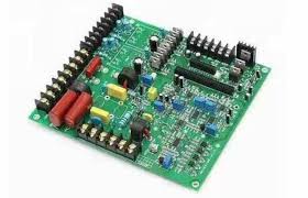
Primary Methods Used in PCB Assembly
Once the components are placed, the PCB is transported to a reflow oven on a conveyor belt. During this step, the paste is heated in a controlled environment to melt it and create secure connections between the components and the PCB. Modern reflow ovens allow for precise control of temperature profiles to ensure consistent and reliable results.
After the reflow process, inspection and quality assurance procedures are conducted to ensure that all components were placed correctly. This can be a time-consuming and labor-intensive task, particularly for complex boards with numerous components. Fortunately, many PCB assembly companies utilize automated testing and inspection processes to speed up the process and minimize the likelihood of errors or defects.
Another important step in the assembly process is x-ray inspection. This is an effective method for screening internal defects in a solder joint. It is non-destructive and identifies defects by the way that they react with x-ray photons. X-rays can detect solder bridging, excessive solder, and other anomalies that may not be visible to the naked eye.
Machines inspect the PCB for soldering defects, component placement issues, and other potential problems using cameras and pattern recognition software. This involves verifying that the assembled PCB performs its intended functions correctly. Tests can include checking for electrical continuity, verifying signal integrity, and simulating real-world operating conditions.