Thermal Dissipation Challenges in HDI PCB Designs
High density interconnect (HDI) represents a major technology trend for advancing contemporary electronic devices. As a critical component in the design and manufacture of these cutting-edge products, understanding the intricacies of this approach to PCB construction is invaluable for engineers and manufacturers committed to maintaining a competitive edge.
As the demand for smaller, more efficient electronic devices continues to grow, HDI technology represents a critical approach to achieving the compact form factor required by many of today’s most demanding applications. This non-conventional method of PCB construction utilizes advanced materials to provide higher pin count connectivity in a smaller space.
Achieving the benefits of HDI requires meticulous engineering. As with all PCB designs, there are numerous challenges that must be addressed to deliver optimal performance. These include complex routing requirements, signal integrity issues, and thermal dissipation concerns.
Procuring an effective solution to these issues requires careful consideration of the layout design and the utilization of appropriate construction techniques. This includes minimizing component size and placement, optimizing layer stacking, utilizing blind and buried vias, and adhering to applicable electromagnetic compatibility (EMI/EMC) standards.
Routing complexities: The tighter spacing between components and traces in an HDI design creates routing congestion, increasing the likelihood of crosstalk and other interference. Careful signal routing and the use of DRC settings in advanced design tools can help to mitigate these difficulties.
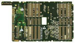
High Density Interconnect and Thermal Dissipation Challenges in HDI PCB Designs
Design complexities: The tighter component placement and layout of an HDI board can introduce a number of manufacturing issues, including misaligned layers and inaccurate drilling. These defects can lead to a host of electrical discontinuities that affect device functionality and reliability.
Thermal dissipation issues: The incredibly thin dielectric material in an HDI design limits the thermal pathways within the circuit board, leading to localized hotspots and elevated temperatures that can compromise a device’s durability and performance. Creating sufficient thermal pathways through the use of copper pours or heat sinks can reduce these risks.
An efficient thermal management strategy is crucial for ensuring proper functionality in an high density interconnect PCB. A proactive approach can mitigate thermal-induced failures and ensure long-term stability for the product. This can be achieved through the use of copper pours, heat sinks, and thermal vias in the circuit board’s stack-up, as well as through the strategic positioning of these features in the layout. The ability to maintain a consistent impedance throughout the circuit board is also essential for ensuring reliable operation. This can be accomplished by using advanced dielectric materials with high thermal conductivity, such as Isola I-Tera MT40.
This material helps to distribute power evenly across the entire board, preventing voltage fluctuations and other failures due to overheating. These strategies can help to address the many thermal-related issues that can arise in an HDI design, preserving its structural resilience and improving its electrical performance. By addressing these challenges, designers can ensure that the full potential of HDI is realized in the final product. This will help to provide reliable electronics that are ready for tomorrow’s exciting applications.